
Views: 0 Author: Site Editor Publish Time: 2026-09-01 Origin: Site


Selecting the right hardware components dictates the success of modern electronic design. This choice directly impacts product footprint, thermal performance, hardware security, and time-to-market. Engineering teams face a constant challenge. They must balance strict performance requirements, such as power efficiency and processing speed, with harsh physical constraints. Software ecosystem dependencies and volatile supply chain realities further complicate the process.
Moving beyond basic definitions requires a rigorous, decision-stage framework. You need to know exactly how to evaluate, categorize, and select these components. This ensures they meet specific application criteria while mitigating implementation risks. A structured approach prevents costly redesigns and ensures long-term field reliability. We will explore the technical dimensions of component selection, focusing on architecture, packaging, power management, and supply chain viability.
Application Dictates Architecture: Selecting between analog, digital, mixed-signal, or security-focused ICs requires mapping exact hardware outcomes to component capabilities.
Packaging is as Critical as Silicon: Thermal dissipation and physical footprint constraints must drive the selection of the IC package type (e.g., BGA, QFN, SOIC), alongside emerging chiplet technologies.
Power Management is a Primary Bottleneck: The integration of a dedicated power management integrated circuit is often mandatory for stabilizing performance in complex, multi-rail systems.
Ecosystem and Supply Chain Viability are Technical Specs: Component lifecycle status, foundry capacity, and manufacturer software support (SDKs/IDEs) must be evaluated alongside electrical specifications to prevent costly redesigns.
An integrated circuit is a miniaturized electronic circuit manufactured entirely on a single semiconductor substrate. This foundational component drives almost all modern electronic devices, replacing bulky discrete transistors, resistors, and capacitors with microscopic equivalents. Success in hardware design starts with understanding the physical and electrical limits of these devices. You must evaluate them based on logic density, switching speed, and power consumption.
A successful implementation meets the target performance metrics without exceeding the allocated thermal or physical budget. For example, replacing a discrete motor control circuit with a single integrated driver reduces the bill of materials (BOM) count, shrinks the PCB area by over 60%, and significantly improves mean time between failures (MTBF) by eliminating dozens of solder joints.
The physical structure dictates the electrical capabilities. The core layers of a Semiconductor IC chip include the silicon substrate, the epitaxial layer, and complex metallization networks. The substrate provides the mechanical foundation and is typically doped to create P-type or N-type semiconductor material. The epitaxial layer hosts the active semiconductor regions where the actual transistors reside. Above this, multiple metallization layers route signals and power between millions of transistors using microscopic copper or aluminum interconnects.
Manufacturing node sizes directly dictate performance limits. Shrinking the node size from 28nm to 5nm increases transistor density. This allows for higher clock speeds and lower dynamic power consumption because the parasitic capacitance of each transistor is reduced. However, smaller nodes increase leakage current, meaning the chip consumes more power even when idle. They also drive up initial manufacturing costs due to the extreme precision required in extreme ultraviolet (EUV) lithography. You must weigh these factors when selecting components for cost-sensitive or battery-powered applications.
A Monolithic IC device integrates all active and passive components onto a single silicon die. Hybrid circuits combine multiple distinct semiconductor dies and discrete passive components onto a shared substrate. Each approach serves different engineering needs.
Monolithic designs offer superior reliability. They eliminate internal interconnects that can fail under thermal stress or mechanical vibration. They also provide the lowest unit cost for high-volume production. However, as die sizes increase, manufacturing yields drop exponentially. A single microscopic defect ruins the entire monolithic die.
Hybrid circuits excel in high-power applications. They allow engineers to mix different semiconductor materials, like Gallium Nitride (GaN) for power switching and standard silicon for logic control. This customization fits niche industrial and aerospace applications perfectly, where a monolithic approach is either impossible or prohibitively expensive.
Advanced packaging now bridges the gap between these two approaches. Chiplet technology and 2.5D/3D integration overcome the yield limits of massive monolithic dies. By breaking a large design into smaller, high-yield chiplets and connecting them via a silicon interposer, manufacturers achieve high-performance computing metrics while keeping production costs manageable. This approach is now standard in high-end server processors and advanced networking hardware.
Digital components process discrete binary values. Microprocessors, FPGAs, and memory chips fall into this category. When evaluating digital parts, focus on clock speed, logic gate count, I/O density, and instructions per clock (IPC). You must also consider setup and hold times to ensure data integrity across different clock domains. High I/O density requires advanced packaging, which complicates PCB routing and often forces the use of expensive high-density interconnect (HDI) boards with blind and buried vias.
Analog components process continuous signals. Operational amplifiers, comparators, and RF transceivers are prime examples. Selection factors here differ entirely from digital parts. You must evaluate signal fidelity, bandwidth, and noise immunity. Key metrics include slew rate, input bias current, and power supply rejection ratio (PSRR). Total harmonic distortion (THD) and common-mode rejection ratio (CMRR) dictate the quality of an analog front end. A poor layout can easily ruin the performance of a high-end analog component by introducing parasitic capacitance or ground loops.
Mixed-signal devices integrate both analog and digital circuits on the same die. They handle tasks requiring Analog-to-Digital Converters (ADC) or Digital-to-Analog Converters (DAC). Use cases include sensor interfacing, precision measurement, and motor control. When selecting an ADC, you must look beyond the stated resolution and evaluate the Effective Number of Bits (ENOB), which accounts for internal noise and distortion. High-resolution mixed-signal devices require careful PCB layout. You must separate analog and digital return paths to prevent high-frequency digital switching noise from corrupting sensitive analog measurements.
Modern hardware requires multiple voltage rails. A processor might need 1.2V for its core, 3.3V for I/O, and 1.8V for memory. A Power management integrated circuit regulates voltage and sequences power across these complex domains. It ensures processors, memory, and sensors receive stable, clean power in the correct order during startup, preventing latch-up conditions.
Evaluating these components requires strict attention to datasheet metrics. Look at conversion efficiency under both heavy and light loads. A switching regulator might boast 95% efficiency at 2A but drop to 60% at 10mA. Quiescent current determines battery life in standby modes. Thermal derating curves show how much current the device can supply as ambient temperature rises. You must also verify fault protection features. Over-Voltage Protection (OVP), Over-Current Protection (OCP), and Under-Voltage Lockout (UVLO) prevent catastrophic hardware failures during abnormal operating conditions.
IoT and enterprise hardware face constant security threats. Trusted Platform Modules (TPMs), Secure Elements, and hardware authenticators provide the necessary defense. These components store cryptographic keys in isolated, tamper-resistant silicon, ensuring that even if the main processor is compromised, the root keys remain secure.
Selection criteria focus on physical and logical defense mechanisms. Look for hardware-level encryption accelerators that offload AES, RSA, or ECC calculations from the main processor, reducing latency and power consumption. Tamper resistance features should include active mesh layers that detect physical probing or decapsulation attempts. Physically Unclonable Functions (PUFs) use microscopic manufacturing variations to generate unique cryptographic keys on the fly, ensuring device authenticity without storing the key permanently in memory.
Application-Specific Integrated Circuits (ASICs) are custom-designed for a single task. General-purpose components, like microcontrollers or FPGAs, handle a wide variety of functions through software or reconfigurable logic. Choosing between them requires analyzing the Return on Investment (ROI) threshold.
Developing a custom ASIC involves massive Non-Recurring Engineering (NRE) costs. You must pay for mask sets, IP licensing, and extensive validation cycles. A single respin due to a design flaw can cost millions of dollars and delay a project by months. However, ASICs offer unmatched power efficiency and unit cost savings at high volumes. You need massive volume requirements—often in the hundreds of thousands or millions of units—to justify ASIC development. For low to medium volumes, off-the-shelf general-purpose components or FPGAs remain the only viable choice.
Managing power and heat dictates system stability. You must calculate total power budgets early in the design phase. This includes dynamic power, which scales with clock frequency and switching activity, and static power, caused by leakage current. Leakage becomes a severe issue at higher operating temperatures, creating a positive feedback loop that can lead to thermal runaway.
Datasheets provide thermal resistance metrics. Theta-JA (θJA) measures thermal resistance from the silicon junction to the ambient air. Theta-JC (θJC) measures resistance from the junction to the component case. You use these metrics to determine cooling requirements. For example, if a component dissipates 2 Watts and has a θJA of 40°C/W, the junction temperature will rise 80°C above ambient. If the ambient temperature is 50°C, the junction hits 130°C. If the absolute maximum rating is 125°C, the design fails. You must implement heatsinks, thermal vias connected to internal copper planes, or active cooling solutions to lower the effective thermal resistance.
Packaging technology impacts physical footprint, manufacturing yield, and mechanical reliability. Through-hole packaging is robust but consumes excessive board space and requires wave soldering. Surface Mount Technology (SMT) dominates modern design, allowing for components on both sides of the PCB.
Package Type | Characteristics | PCB Routing Impact | Best Use Case |
|---|---|---|---|
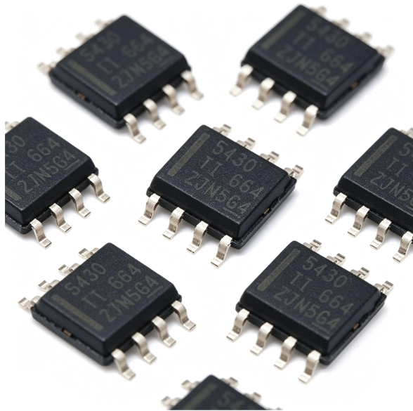
SOIC / TSSOP | Gull-wing leads, easy to inspect visually. | Low complexity, requires fewer PCB layers. | General logic, analog components, low-cost boards. |
QFN (Quad Flat No-lead) | Pads on the bottom, excellent thermal pad. | Moderate complexity, requires thermal vias. | Power management, RF transceivers, motor drivers. |
BGA (Ball Grid Array) | Solder balls under the package, high pin count. | High complexity, requires multi-layer boards and microvias. | Microprocessors, FPGAs, high-speed memory. |
WLCSP (Wafer-Level Chip Scale Package) | Die-sized package, absolute minimum footprint. | Very high complexity, tight trace tolerances. | Mobile devices, wearables, ultra-compact IoT. |
Packaging directly affects mechanical reliability. Boards subjected to heavy vibration or thermal cycling require packages that absorb mechanical stress. The Coefficient of Thermal Expansion (CTE) mismatch between the silicon die, the package substrate, and the FR4 PCB causes stress on solder joints during temperature changes. Leaded packages like SOIC handle board flex better than rigid QFNs. BGA packages require careful underfill processes in high-vibration environments to prevent solder joint fractures.
Hardware capabilities mean nothing without software access. You must evaluate the manufacturer's software ecosystem before committing to a part. Assess the availability and maturity of Software Development Kits (SDKs), Integrated Development Environments (IDEs), and reference designs. Check if the manufacturer provides a robust Hardware Abstraction Layer (HAL) to speed up peripheral configuration.
A superior hardware component will bottleneck your project if it has poor firmware support. Lack of Real-Time Operating System (RTOS) compatibility delays development. Undocumented silicon errata can cause random system crashes that take weeks to debug. Always review community forums, GitHub repositories, and support portals to gauge the actual quality of the toolchain. If the manufacturer relies on an outdated, Eclipse-based IDE that crashes frequently, your firmware team will lose hundreds of hours in lost productivity.
Operating environments dictate component selection. Industry-specific reliability standards ensure components survive their intended use cases. The AEC-Q100 standard dictates stress testing for automotive applications, categorizing parts into grades based on temperature tolerance (e.g., Grade 1 for -40°C to +125°C). MIL-PRF-38535 covers aerospace and defense requirements, often mandating hermetic ceramic packaging and radiation tolerance. Medical devices follow strict ISO standards for safety and reliability, requiring extensive documentation and traceability.
Operating temperature ranges severely impact component lifespan. Commercial grade parts typically operate from 0°C to 70°C. Industrial grade parts extend this from -40°C to 85°C. Automotive grades can reach up to 150°C. Pushing a component beyond its rated temperature accelerates electromigration, where the flow of electrons physically moves metal atoms within the chip's interconnects, eventually leading to open or short circuits and premature failure.
Unit economics shift drastically as a project moves from prototype to production. Prototyping relies on distributor pricing, which carries high margins. You buy small quantities from catalogs in cut-tape format to build initial test boards. Cost is secondary to availability at this stage. You need the parts on your desk tomorrow to begin validation.
High-volume production requires direct manufacturer negotiations or working through franchised distributors for volume pricing. You buy parts in full tape-and-reel format for automated pick-and-place assembly. This introduces Minimum Order Quantities (MOQs) and strict delivery schedules. You must forecast demand accurately to avoid tying up capital in excess inventory or halting production due to component shortages. You must also account for attrition rates during assembly, as pick-and-place machines will inevitably drop or misplace a small percentage of components.
Understanding the semiconductor supply chain helps anticipate macro-level constraints. The industry separates design from manufacturing. Fabless companies design the chips but do not own manufacturing facilities. They contract foundries to fabricate the silicon wafers.
This model creates fab capacity bottlenecks. When global demand spikes, foundries prioritize high-margin, high-volume customers. Smaller fabless companies face extended lead times, sometimes stretching from 12 weeks to over 52 weeks. You must track foundry capacity trends and raw material availability to anticipate when your selected components might face allocation issues.
Supply chain risks can kill a product before it launches. You need strict mitigation strategies. Always check the lifecycle status of a component. Avoid parts marked "Not Recommended for New Designs" (NRND) or "End of Life" (EOL). These parts will soon disappear from the market, forcing a costly PCB redesign and software port.
Identify pin-to-pin drop-in replacements early in the design phase. This allows you to swap parts without redesigning the PCB if the primary component becomes unavailable. Dual-sourcing critical components protects against geopolitical factors, factory fires, and raw material shortages that disrupt long-term availability. Pay attention to Product Change Notifications (PCNs) from manufacturers, which alert you to changes in the manufacturing process or die revisions that might affect your product's performance.
High-speed integration introduces severe signal integrity risks. Fast edge rates cause crosstalk between adjacent traces due to parasitic capacitive and inductive coupling. Impedance mismatches reflect signals back down the line, causing ringing and data corruption. Electromagnetic Interference (EMI) emissions can cause your product to fail regulatory compliance testing (FCC/CE), preventing you from legally selling the device.
Mitigation requires strict adherence to datasheet layout guidelines. Maintain continuous ground planes under high-speed signals to provide a clear, low-impedance return path. Never route high-speed signals over a split in the ground plane, as this creates a massive loop antenna. Place decoupling capacitors as close to the power pins as physically possible, prioritizing the smallest value capacitors closest to the pin. This minimizes loop inductance and suppresses high-frequency switching noise. Use proper via stitching around the board perimeter to contain EMI within the board structure.
Never design a custom PCB without validating the core components first. Use manufacturer evaluation boards (eval kits) to test performance claims. This proves the software toolchain works, verifies power consumption metrics under real loads, and allows the firmware team to begin development months before the custom hardware arrives.
Post-assembly quality control ensures manufacturing defects do not reach the field. Implement boundary scan (JTAG) to test internal connections between ICs without requiring physical test probes on every net. Automated Optical Inspection (AOI) catches missing components, tombstoning, and solder bridges on visible pins. X-ray inspection is mandatory for BGA and QFN packages to verify solder joint integrity and detect voiding hidden beneath the component body.
Download and review the complete datasheets, application notes, and silicon errata documents for all shortlisted components.
Order manufacturer evaluation boards to validate power consumption profiles and software toolchain compatibility before beginning schematic capture.
Identify and document at least one pin-to-pin compatible alternative for critical logic and power management components to secure the supply chain.
Consult with a specialized electronics manufacturing service (EMS) partner for a Design for Manufacturing (DFM) review to verify PCB layout constraints and assembly tolerances.
A: A microprocessor is a specific type of complex digital component designed to execute software instructions and process data. A standard component is a broader category that includes simple logic gates, analog amplifiers, and memory chips. All microprocessors are integrated circuits, but not all integrated circuits are microprocessors.
A: Package selection depends on thermal dissipation, physical space, and PCB manufacturing capabilities. Use QFN packages for good thermal performance in tight spaces. Choose BGA for high-pin-count microprocessors, though it requires expensive multi-layer PCBs. Use SOIC for simple logic where low-cost, two-layer PCB routing is preferred.
A: A PMIC regulates and distributes power across multiple voltage rails within a system. It handles voltage conversion, power sequencing during startup, and battery charging. It also provides critical fault protection, including over-voltage, over-current, and thermal shutdown, ensuring system stability under varying load conditions.
A: Operating temperatures dictate the required component grade. Commercial parts operate from 0°C to 70°C. Industrial parts handle -40°C to 85°C, and automotive parts withstand up to 150°C. Exceeding these ratings causes thermal runaway, accelerates electromigration, and leads to permanent physical damage to the silicon die.
A: NRND indicates that the manufacturer plans to phase out the component soon. While the part is currently in production, it will eventually transition to End of Life (EOL). You should never use NRND parts in new hardware designs, as future supply chain availability cannot be guaranteed.
A: The hardware cannot function without code. A poor software ecosystem lacks reliable SDKs, IDEs, and documentation. This delays firmware development, complicates RTOS integration, and makes debugging silicon errata nearly impossible. A mature toolchain accelerates time-to-market and ensures stable field performance.


